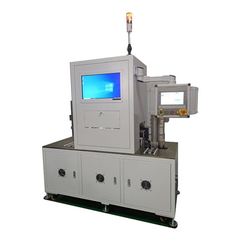
Solid state wire bonding AOI inspection machine, also known as wire bonding AOI inspection machine, is mainly used for efficient AOI inspection of defects after die bonding and wire bonding in the semiconductor packaging and testing field. It has the characteristics of high speed, high precision, and high inspection coverage. Optical system modules and core detection algorithms with completely independent intellectual property rights, as well as AI deep learning algorithms, are suitable for detecting various defects on grain surfaces, solder joints, solder wires, and frame surfaces that occur during the solidification and wire bonding processes.
|
Project |
Performance index |
|
|
Application area |
IC field, power devices (IGBT, etc.), SIP, discrete devices, COB, optical communication field, lighting LED MiniLED、MicroLED、 Lead frame, etc |
|
|
Detection range |
Grain detection |
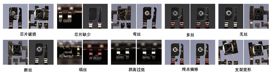
Detection of missing grains, angles, sizes, positions, chipping, scratches, cracks, overlaps, foreign objects, dirt, surface coatings, etc |
|
Solder joint detection |
Solder joint size, offset, virtual soldering, wire warping, etc |
|
|
Wire detection |
Missing gold wire, collapsed wire, inverted wire, broken wire, bent wire, re welding, line width, high arch height, low arch height, etc |
|
|
Adhesive/solder testing |
Glue coverage, offset, overflow, grain surface on glue, tail pulling, solder splashing, bridging and tin sticking, bubbles inside the glue, impurities, etc |
|
|
Framework/Pin Detection |
Frame/pin connections, defects, bends, dirt, foreign objects, etc |
|
|
Optical system |
5-megapixel color industrial camera with a resolution of 15um |
|
|
Far center lens+customized combination light source |
||
|
Sports organization |
Track type fully automatic loading and unloading conveyor, with a track width of 40-70mm that can be automatically adjusted for tray or sheet operation, and the track width can be customized |
|
|
The movement of the material tray or sheet in the track is carried out by a screw module and driven by a motor |
||
|
Support automatic line stringing or automatic loading and unloading, automatic loading and unloading support multiple forms and specifications, can be selected or partially customized according to product or vehicle specifications |
||
|
Software system |
1. Humanized operation interface, users can set access permissions for different groups according to their needs (unlimited number of groups); 2. It has detailed historical batch detection information, as well as missing path analysis and measurement analysis functions; 3. Mapping information for defects can be provided to subsequent processes in formats such as CSV files, TXT text, HTML files, HTTP API requests, and SQLite data files; 4. When the device alarms, the interface displays information clearly and has the function of recording and querying historical alarm information; |
|
|
Data management |
Data analysis tools, including historical data queries, yield analysis, defect statistics, and mapping defect distribution, etc |
|
|
Laser burn off |
The laser module is integrated into existing equipment, and for defective products detected during inspection, laser burning treatment is carried out |
|
Defect image
This device measures the thickness of wafers and display panels after partial processes such as wafer slicing, grinding, thinning, and slicing. Can synchronously test the TTVBOWWRAP/SORI and other parameter errors of the material itself.
View More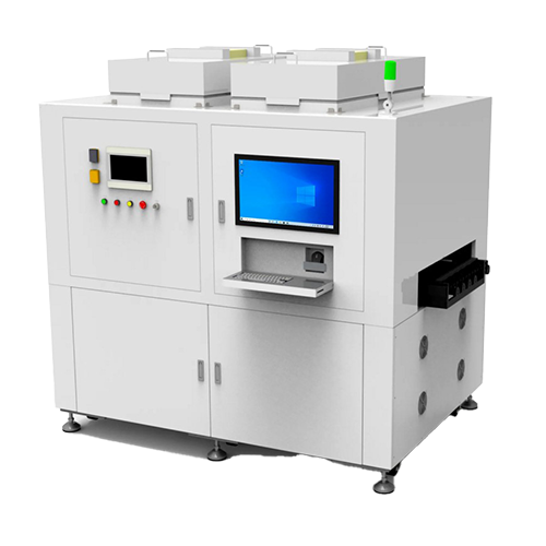
The wafer scratch AOI inspection machine is mainly used for detecting obvious scratch defects such as missed scratches, defocusing, uncut, and bicrystals on the core grains on the Disco ring after wafer splitting machine processing. Through Machine Vision defect detection, the presence or absence of the above defects can be detected to distinguish between good and defective products, reduce manual labor, and improve detection efficiency.
View More
Solid state wire bonding AOI inspection machine, also known as wire bonding AOI inspection machine, is mainly used for efficient AOI inspection of defects after die bonding and wire bonding in the semiconductor packaging and testing field. It has the characteristics of high speed, high precision, and high inspection coverage. Optical system modules and core detection algorithms with completely independent intellectual property rights, as well as AI deep learning algorithms, are suitable for detecting various defects on grain surfaces, solder joints, solder wires, and frame surfaces that occur during the solidification and wire bonding processes.
View More
The shape and distribution of dislocation defects in semiconductor wafer preparation have a significant impact on the performance of electronic components. Due to differences in doping materials and preparation processes, the distribution of dislocations also varies. This device is used to inspect the morphology and distribution of wafer dislocations, providing data support for wafer material research and improving preparation processes. Suitable for 2-inch, 3-inch, 4-inch, and 6-inch gallium arsenide substrates.
View More Address:Unit 204, No. 30 Guanri Road, Phase II Software Park, Xiamen City
Factory Address:1st Floor,Great Wall Business Building,76-78 Huli Avenue,Xiamen City
Address:Unit 204, No. 30 Guanri Road, Phase II Software Park, Xiamen City
Factory Address:1st Floor,Great Wall Business Building,76-78 Huli Avenue,Xiamen City
 Consultation Hotline:86-0592-3799658、86-137 9991 1773(Switchboard)
 Email : AOI@otek.com.cn